Performance Tuning Parameters
Several parameters are provided to allow tuning of the performance. These parameters fall into three broad categories; bandwidth allocation, packet blocking optimization, and tag scan rates.
Bandwidth Allocation Parameters
Bandwidth can be allocated for the different types of data as desired. The parameters to perform this are as follows:
|
[Parameter] |
[Default Value] |
[Parameter Type] |
|---|---|---|
|
25 |
integer |
|
|
12 |
integer |
|
|
13 |
integer |
|
|
50 |
integer |
The percentage bandwidth allocated to each queue will be the ratio of an individual queue's value when compared to the total sum of defined bandwidths. The default values have a sum of 100 for ease of reference. Any unused bandwidth will be shared amongst the other categories.
Bandwidth can be configured at the port level, but not the device level.
Example:
[SEPAM40]
EventsBandwidth 30
WaveformsBandwidth 5
CommandsBandwidth 15
RealTimeBandwidth 50
[SEPAM40.MYCLUSTER.PORT_1]
EventsBandwidth 50
WaveformsBandwidth 30
CommandsBandwidth 10
RealTimeBandwidth 10
BandwidthAllocation
This parameter allows the ratio of bandwidth assigned to each device sharing a port to be configured. This parameter can only be configured at the device level.
Parameter type: integer
Default value: <equal split>
Example:
[SEPAM40.MYCLUSTER.PORT_1.DEVICE_A]
BandwidthAllocation 70
[SEPAM40.MYCLUSTER.PORT_1.DEVICE_B]
BandwidthAllocation 30
Packet Blocking Optimization Parameters
For all devices except the Sepam, parameters can be configured to optimize the MODBUS packets that are created for collection of data from the device. Sepam devices have pre-configured blocks that are already optimized.
The parameters that control the blocking are as follows:
enableScatteredReads
This causes the driver to use the ‘scattered read’ extension that can help improve blocking. This option should be enabled for devices that support this extension.
Parameter type: Boolean flag
Default value: 0 for generic Power MODBUS driver, 1 for PowerLogic driver
Example:
[PWRMODBUS.MYCLUSTER.PORT_1.DEVICE_A]
enableScatteredReads 1
[PWRMODBUS.MYCLUSTER.PORT_1.DEVICE_B]
enableScatteredReads 0
percentBlockFill
This parameter defines the maximum percentage of configured registers contained in a block before the drivers creates fixed blocks instead of scattered blocks. The following figure illustrates now a block of N registers can be constructed:
- If M<N registers are configured, the block builder can either create a scattered block or a multi-register block.
- If M/N*100% is less than PercentBlockFill, the block builder creates a scattered registers block.
- If the percentage of configured registers ≥ PercentBlockFill, the block builder creates a multi-register block.
Parameter type: percentage
Default value: 50
Example:
[PM870.MYCLUSTER.PORT_1.PM_DEVICE]
percentBlockFill 50
[CM4000.MYCLUSTER.PORT_1.CM_DEVICE]
percentBlockFill 80
maxBlockSize
This parameter defines the maximum number of registers that can be read in a single request. By default, this is 124, but some devices can read more than this.
Parameter type: integer
Default value: 124
Example:
[PWRMODBUS.MYCLUSTER.PORT_1.DEVICE_A]
maxBlockSize 1024
minBlockSize
This parameter defines the minimum number of registers to read as a fixed block before the block builder will instead add those registers to a scattered block. If latency is low, and scattered reads are expensive, this value should be lower. If latency is high, or scattered reads are inexpensive, it is better to set this value higher. Only applicable when scattered reads are enabled.
Parameter type: integer
Default value: 20
Example:
[PM870.MYCLUSTER.PORT_1.LOW_LATENCY_DEVICE]
minBlockSize 10
[CM4000.MYCLUSTER.PORT_1.HIGH_LATENCY_DEVICE]
minBlockSize 100
Tag Scan Rate Parameters
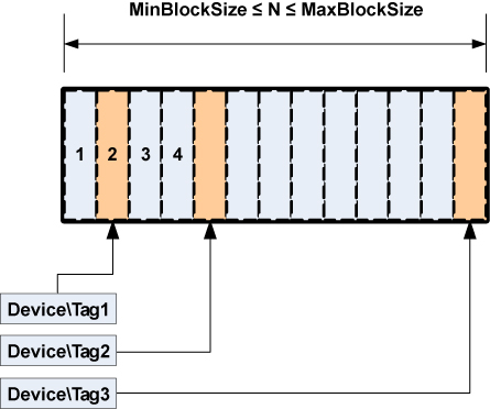
Each tag can be configured at a priority level from 1-3 where 1 is the highest. Parameters exist to adjust the relative scan rates of the high and low priority tags in comparison to the nominal tag scan rate.
HighScanRate
Parameter type: percent relative to nominal
Default value: 50
LowScanRate
Parameter type: percent relative to nominal
Default value: 200
Using the default parameters, the high priority tags will be refreshed twice as fast as the normal priority tags, and the low priority tags will be refreshed at half the rate of the normal priority tags. These parameters can be configured at the port level and higher.
Using the default settings and a nominal tag refresh rate of 1 second:
Low Priority Tag Refresh: 2000 ms
Normal Priority Tag Refresh: 1000 ms
High Priority Tag Refresh: 500 ms
Example:
[PM870.MYCLUSTER.PORT_1]]
HighScanRate 25
LowScanRate 500T
Advanced Tag Block Capabilities (Invalid Memory Access Blocks defined)
Some devices may restrict access to certain memory registers. Such registers may be available for read only, write only or may not be available at all, resulting in a MODBUS exception when the registers are addressed.
Definition: Blocks of registers that cannot be read or written to are referred as “invalid memory access blocks.”
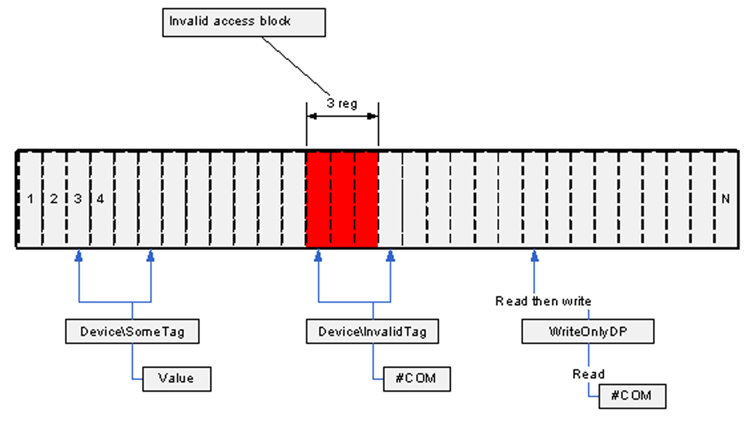
These devices create a challenge for the PWRMODBUS driver. If the device has invalid blocks that do not support scattered reads (or they are disabled for this device), the driver may try to read registers in blocks that intersect with the registers that cannot be read. This can result in the whole block being invalidated and, in certain cases, may also result in device being taken offline. Figure 1 (below) illustrates an invalid block in the middle of an address space.
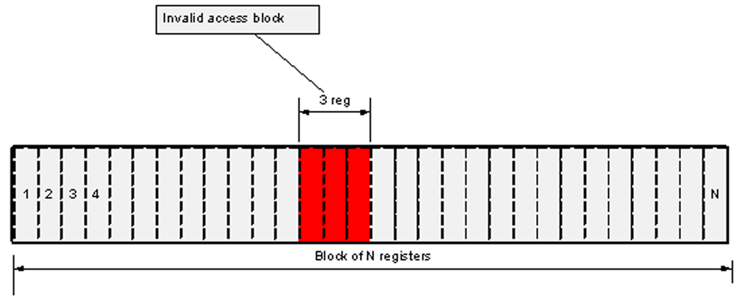
Figure 1 shows how the "invalid memory access block" affects MODBUS register blocking. In this situation, if the driver does not know that the block of 3 inaccessible registers exists, it will try to block all registers from 1 to N (depending on data that was requested by the real-time data collector). This block, however, will never be read successfully, as the device will respond with an exception to all attempts to read invalid registers.
If the configuration includes information about invalid memory access blocks, the driver will create two blocks instead of one, as shown in Figure 2:
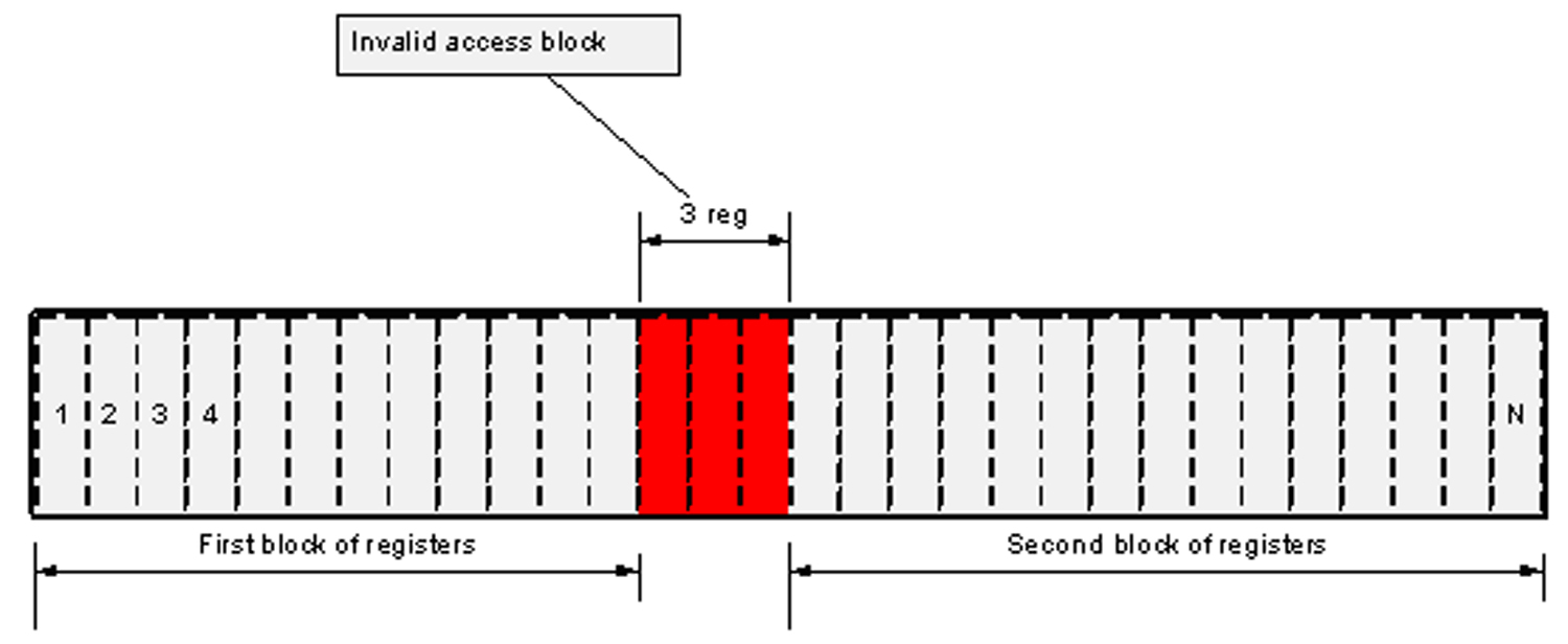
In Figure 2, invalid registers were taken into account when the block was constructed. When configuring device that has invalid memory areas, it is especially important to define all blocks that may interfere with any of the tags.
Invalid Block Tag Definition Syntax
Invalid access memory areas are defined as variable tags, using the following format for the address:
T:IB;{m|i|c|s}:<start_register>:u<count>;E:1;L:P:0
where
• m, i, c and s define the type of MODBUS register
• <start_register> is the first register address of the invalid access block
• <count> defines the number of registers in the invalid access block
Example:
T:IB;m:300:u10;E:1;L:P:0
This defines an invalid access block of ten holding registers starting from register 300.
Configuration Notes
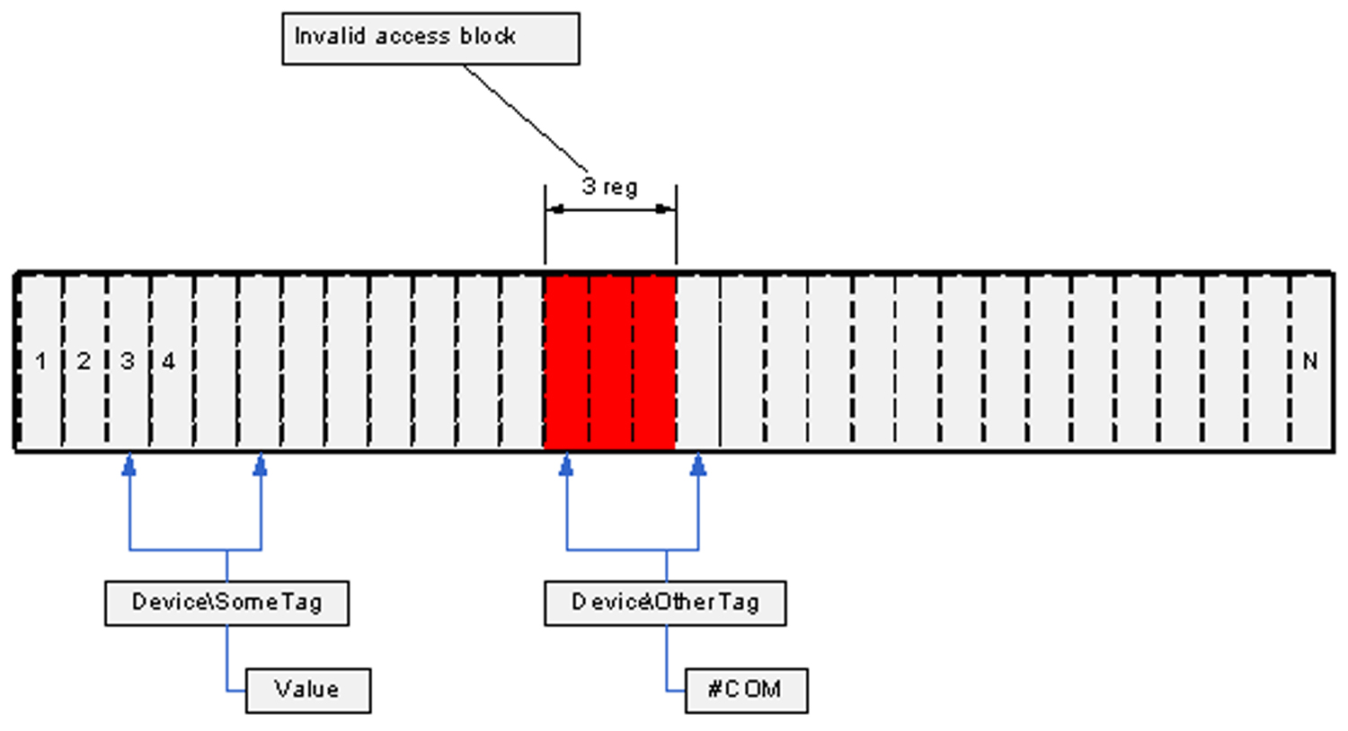
When one or more invalid access blocks is defined according to the syntax described in Invalid Block Tag Definition Syntax, tags configured to read any of invalid registers will be affected by it. If any of the tag registers fall into an invalid memory access block, this tag will not be readable; any attempt to read its value will result in #COM, as shown on Figure 3:
However, such tags do not affect other tags, because the PWRMODBUS driver implements algorithms that prevent tags from being invalidated by invalid memory block logic.
Tags that try to use invalid registers are detected on startup and can be found by analyzing the log file. This is an example trace:
[DEBUG] [REAL][GeneralDriver::BaseDatapointBuilder::BuildDataPoints()] Adding datapoint. Tag - BCM1\H_QIVR34\SwlStr Address - T:SS;m:283:2;E:1;L:P:26 Datapoint: class Datapoints::Status_SS
[DEBUG] [REAL][RealTimeData::DeviceCache::Subscribe()] Init Registers: Polled Registers: Address:283 Type:3
[ERROR] [MISC] [RealTimeData::BlockBuilder::AddDataPoint()] Cannot add datapoint, one or more invalid memory addresses fall into non-splittable block
[ERROR] [MISC] [GeneralDriver::BaseDatapointBuilder::BuildDataPoints()] Could not init datapoint. Tag BCM1\H_QIVR34\SwlStr Address T:SS;m:283:2;E:1;L:P:26. Analyze other messages, this tag address may contain invalid registers
Such output is expected when a holding register with address 283 is declared invalid. This trace helps figure out any configuration issues.
Write-only Memory
If a certain register range is accessible for write only, no additional configuration may be needed. However, to prevent the driver block optimizer from including these registers in a poll, they also must be configured by adding “invalid block” tags as described in the Invalid Block Tag Definition Syntax, described previous. Declaring these registers invalid will not prevent drivers from trying to write to them. Figure 4 illustrates a write-only memory configuration:
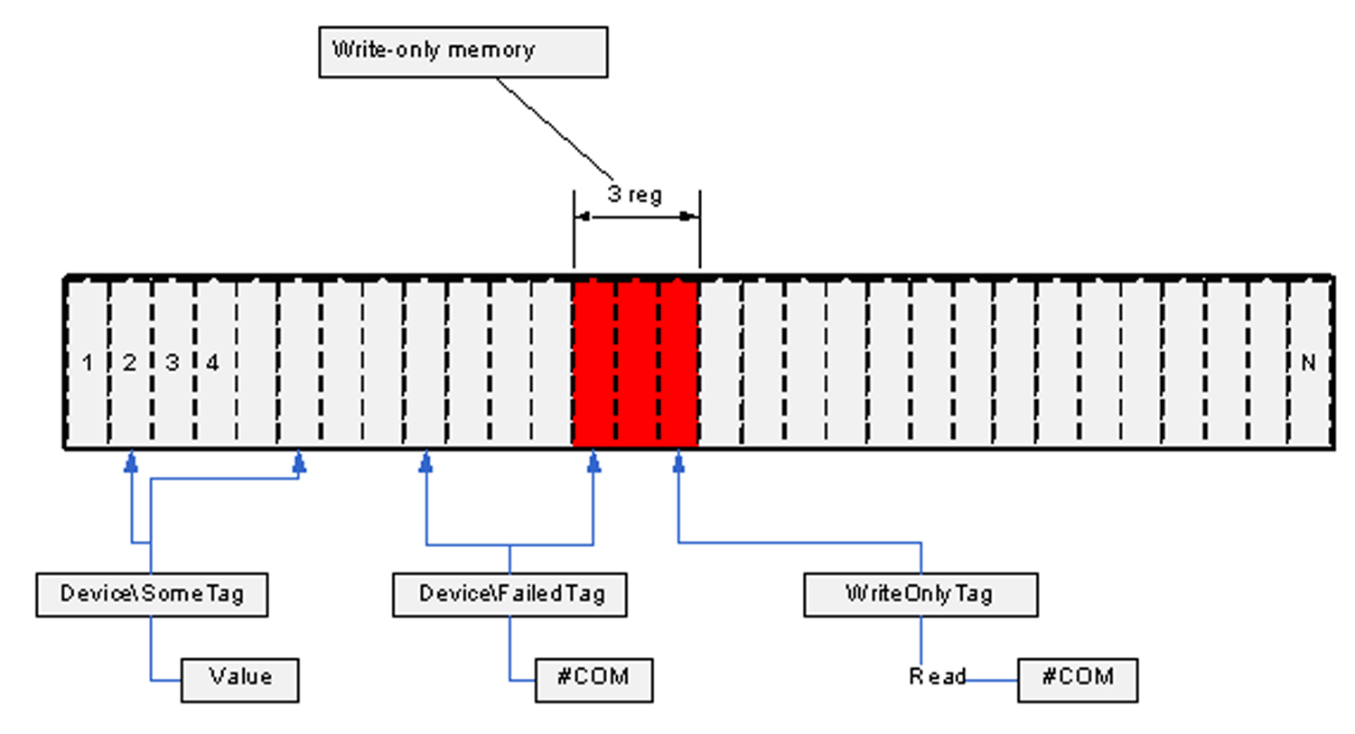
Write-only registers should not be confused with write-only datapoints that internally read a register before attempting to write. Declaring the register they read invalid will result in a datapoint not working; such mistake should be avoided. Figure 4 shows “WriteOnlyDP” as an example; this tag cannot be read (it will result in #COM), but internally it needs to get the register value before writing into it. If this register was declared invalid, tag writes would also not succeed.
Figure 5 illustrates a write-only datapoint:
Tag Blocking Notes
The drivers support an advanced blocking mechanism for tags. That is, real-time tags are no longer blocked together with write-only tags.
Tags found invalid, due to intersection with invalid memory areas, are not blocked with “good” real-time tags and will not therefore interfere with them.
Write-only Tags
Beginning with driver version 2.0.1.1, the write-only tags feature is fully supported.
There are no special logic codes or address formats for write-only tags. If a tag references memory that was declared invalid (see Invalid block tag definition syntax, previous), and its datapoint has writing capabilities, the tag becomes write only. No preliminary checks are performed to verify that the memory can be written to, and no additional configuration is needed. It is assumed that, if the tag is configured to write into memory that has been declared “invalid,” the memory can actually be written to.
It is important to understand that scaled write tags (code 110) will become write-only tags, if that scale register can be read. Tag Device\TagN on Figure 6 explains this case: the datapoint needs to read the scale value from the scale register in order to write scaled value to write-only register. However, as long as the actual register belongs to the memory that can only be written to (and it is configured using T:IB tag syntax as explained in Invalid Block Tag Definition Syntax previous), this tag cannot be read.
The fact that the tag mentioned before cannot be read will not affect other tags reads (see Tag Blocking Notes, previous).
NOTE: The write-through feature of the device cache is disabled for write-only tags.