TM3DQ16T / TM3DQ16TG Characteristics
This section provides a description of the electrical and the output characteristics of the TM3DQ16T / TM3DQ16TG expansion modules.
See also Environmental Characteristics.
|
|
|
UNINTENDED EQUIPMENT OPERATION |
|
Do not exceed any of the rated values specified in the environmental and electrical characteristics tables. |
|
Failure to follow these instructions can result in death, serious injury, or equipment damage. |
The following diagrams show the external dimensions for the TM3DQ16T / TM3DQ16TG expansion modules:
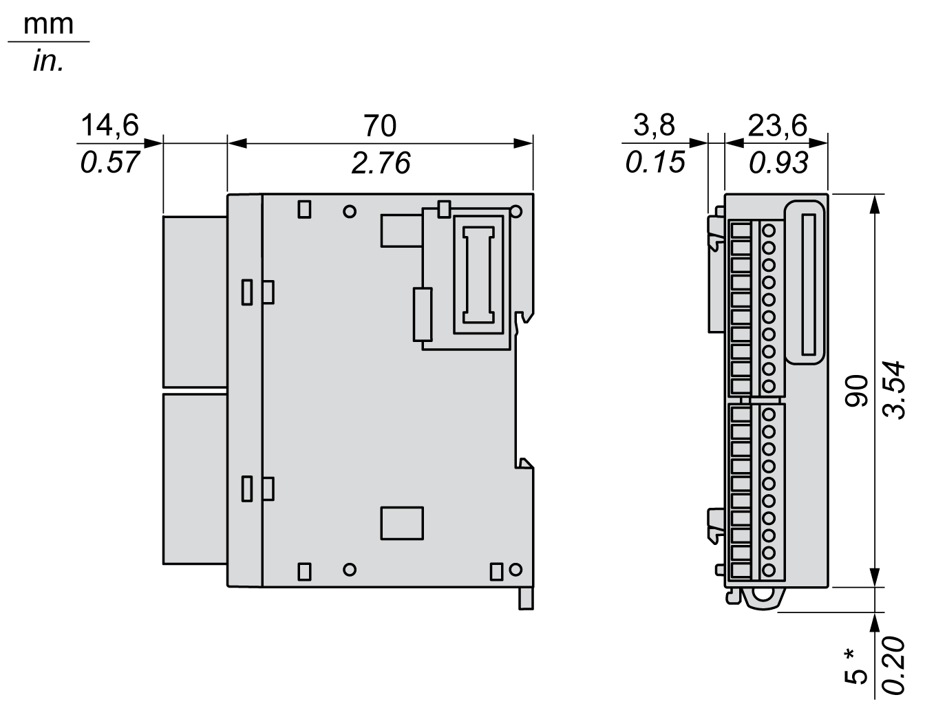
* 8.5 mm (0.33 in) when the clamp is pulled out.
The table below describes the outputs characteristics of the TM3DQ16T and TM3DQ16TG
|
Characteristic |
Value |
|
|---|---|---|
|
Number of output channels |
16 |
|
|
Number of channel groups |
1 common line on 2 terminals for 16 channels |
|
|
Output type |
Transistor |
|
|
Logic type |
Source |
|
|
Rated output voltage |
24 Vdc |
|
|
Output voltage range |
19.2...28.8 Vdc |
|
|
Rated output current |
0.5 A |
|
|
Total output current per group |
8 A |
|
|
Voltage drop |
0.4 Vdc max. |
|
|
Leakage current when switched off |
0.1 mA max. |
|
|
Maximum power of filament lamp |
3 W |
|
|
Inductive load |
L/R = 10 ms |
|
|
De-rating |
- 10...55 °C (14...131 °F) |
No de-rating |
|
Turn on time |
450 µs |
|
|
Turn off time |
450 µs |
|
|
Protection against short circuit |
Yes |
|
|
Short circuit output peak current |
1 A typically |
|
|
Automatic rearming after short circuit or overload |
Yes, time depending on component temperature |
|
|
Protection against reverse polarity |
Yes |
|
|
Clamping voltage |
Typically 50 Vdc |
|
|
Switching frequency |
Under resistive load |
100 Hz max. |
|
Isolation |
Between output and internal logic |
500 Vac |
|
Between channel group |
N/A |
|
|
Connection type |
TM3DQ16T |
Removable screw terminal blocks |
|
TM3DQ16TG |
Removable spring terminal blocks |
|
|
Connector insertion/removal durability |
Over 100 times |
|
|
Current draw on 5 Vdc internal bus |
20 mA (all outputs on) 5 mA (all outputs off) |
|
|
Current draw on 24 Vdc internal bus |
16 mA (all outputs on) 0 mA (all outputs off) |
|
|
NOTE: Refer to Protecting Outputs from Inductive Load Damage for additional information concerning output protection. |
||
