The TM5SAI2H and TM5SAI4H expansion electronic modules are 10 Vdc Analog Input electronic modules with 2 and 4 inputs respectively.
If you have wired your input for a voltage measurement and you configure EcoStruxure Machine Expert for a current type of configuration, you may permanently damage the electronic module.
|
NOTICE |
|
INOPERABLE EQUIPMENT |
|
Verify that the physical wiring of the analog circuit is compatible with the software configuration for the analog channel. |
|
Failure to follow these instructions can result in equipment damage. |
For further information, refer to the Hardware Guide:
|
Reference |
Refer to |
|---|---|
|
TM5SAI2H |
|
|
TM5SAI4H |
The user can specify an upper and lower limit value for each individual channel.
When activated, the input signals are monitored to see if the limit values are exceeded. The defined limit values are used for this. If the analog value goes beyond the defined range, then it is limited to the upper or lower limit value.
The result of the signal check is displayed in a corresponding status bit. If necessary, the counters are incremented by one if the value falls outside the range.
The raw A/D converter data and the filtered A/D converter data are compared. The system measure and the user measure are grouped internally as a k/d pair to optimize the execution time. Gain and offset can be specified for each individual channel.
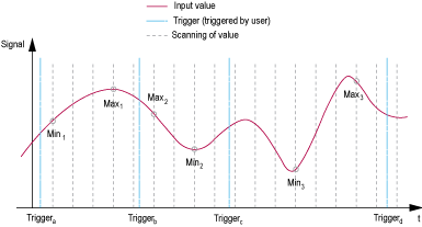
Minimum and Maximum Input Values
The system stores the minimum and maximum values between two trigger events. The function is started by the corresponding trigger edge. The following edges are evaluated depending on the configuration:
oPositive edge
oNegative edge
oPositive and negative edge
The trigger counter counts valid trigger events. In the event that trigger events occur faster than the sampling cycle, the triggering becomes invalid (trigger detected error counter is incremented).
The following example shows how the minimum and maximum input values are recorded:
|
Trigger Event |
Description |
|---|---|
|
Trigger a |
The function is started. The system notes the minimum and maximum values of the input signal. Ignore the Min./Max values registered by the status bit after the initial start. |
|
Trigger b |
The minimum value (Min1) and the maximum value (Max1) between Trigger a and Trigger b are given to the register and the new cycle is started. A status bit informs the user as soon as the values are valid. |
|
Trigger c |
The minimum value (Min2) and the maximum value (Max2) between Trigger b and Trigger c are given to the register and the new cycle is started. A status bit informs the user as soon as the values are valid. |
|
Trigger d |
The minimum value (Min3) and the maximum value (Max3) between Trigger c and Trigger d are given to the register and the new cycle is started. A status bit informs the user as soon as the values are valid. |
The electronic module has an Input cycle that can be configured separately for each individual channel. The order and cut-off frequency can be specified for each individual channel:
oFilter Order: 1...4 (default: 1)
oFilter Cut-off frequency: 1...65535 Hz (default: 500 Hz)
Variables can be defined and named in the TM5 Module I/O Mapping tab. Additional information such as topological addressing is also provided in this tab.
This table describes the I/O mapping configuration:
|
Channel |
Type |
Description |
|---|---|---|
|
ModuleOK |
BYTE |
State of the compact I/O and electronic modules |
|
DcOk |
BOOL |
Voltage range: o0: Invalid o1: Valid |
|
reserved |
BOOL |
Reserved. |
|
NetworkOk |
BOOL |
TM5 bus: o0: Bus error o1: OK |
|
I/O Data valid |
BOOL |
Data validity: o0: Valid o1: Invalid |
|
reserved |
BOOL |
Reserved |
|
reserved |
BOOL |
Reserved |
|
reserved |
BOOL |
Reserved |
|
reserved |
BOOL |
Reserved |
|
Status |
Status |
BYTE |
State of all inputs |
|
|
|
Status Analog Input 01 |
BOOL |
Status of analog inputs: o0: Ok. o1: Error |
|
|
... |
... |
|||
|
Status Analog Input 04 |
Status of analog inputs: o0: Ok. o1: Error |
|||
|
reserved |
reserved |
|||
|
reserved |
reserved |
|||
|
synchronisation TM5 to conversion cycle |
Synchronisation TM5 to conversion cycle: o0: Synchronisation ok o1: Synchronisation error |
|||
|
Conversion Cycle |
Status conversion cycle: o0: Ok o1: Error |
|||
|
Inputs |
AnalogInput00 |
INT |
Current value of input 0 |
|
|
... |
... |
|||
|
AnalogInput03 |
Current value of input 3 |
|||
For further generic descriptions, refer to User-Defined Parameters Tab Description.
This table describes the TM5SAI2H and TM5SAI4H user-defined parameters configuration:
|
Name |
Value |
Default Value |
Description |
|---|---|---|---|
|
ChannelFilter01 |
off on |
off |
Enables/disables the channel filter. |
|
MinMaxCheck01 |
off positive |
off |
Activates the minimum and maximum channel values. |
|
ChannelErrCheck01 |
off on |
on |
Detects an error on the channel. |
|
ChannelType01 |
-10 V to +10 V 0 to 20 mA |
-10 V to +10 V |
Specifies the channel type. |
|
MinLimit01 |
-32768...32767 |
-32767 |
|
|
MaxLimit01 |
-32768...32767 |
32767 |
|
|
UserGain01 |
-2,147,483,648...2,147,483,647 |
65536 |
The user-defined gain for the A/D converter data of the respective physical channel can be specified in these registers. The value 65536 (0x10000) corresponds to a gain of 1. |
|
Useroffset01 |
-2,147,483,648...2,147,483,647 |
0 |
The user-defined offset for the A/D converter data of the respective physical channel can be specified in this register. The value 65536 (0x10000) corresponds to an offset of 1. |
|
FilterOrder01 |
1...4 |
1 |
Filter order selection. |
|
FilterConstant01 |
1...65535 |
500 |
Cutoff frequency in Hertz. |
|
... |
|
|
|
|
ChannelFilter04 |
off on |
off |
Enables/disables the channel filter. |
|
ChannelErrCheck04 |
off on |
on |
Detects an error on the channel. |
|
ChannelType04 |
-10 V to +10 V 0 to 20 mA |
-10 V to +10 V |
Specifies the channel type. |
|
MinLimit04 |
-32768...32767 |
-32767 |
|
|
MaxLimit04 |
-32768...32767 |
32767 |
|
|
UserGain04 |
-2,147,483,648...2,147,483,647 |
65536 |
The user-defined gain for the A/D converter data of the respective physical channel can be specified in these registers. The value 65536 (0x10000) corresponds to a gain of 1. |
|
Useroffset04 |
-2,147,483,648...2,147,483,647 |
0 |
The user-defined offset for the A/D converter data of the respective physical channel can be specified in this register. The value 65536 (0x10000) corresponds to an offset of 1. |
|
FilterOrder04 |
1...4 |
1 |
Filter order selection. |
|
FilterConstant04 |
1...65535 |
500 |
Cutoff frequency in Hertz. |
|
SampleTime |
50...10000 |
100 |
The sampling time is set to µs in this register. This makes it possible to improve the sampling cycle (resolution = 1 µs). The lowest configurable cycle time is 50 µs. |