Signals
Logic Type
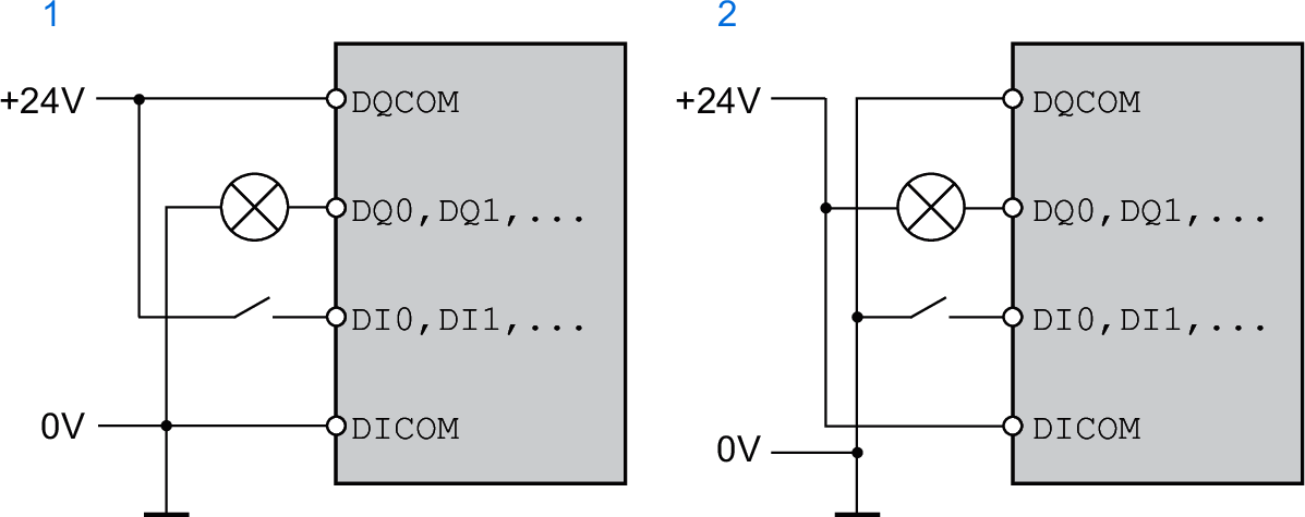
The digital inputs and outputs of this product can be wired to enable positive logic or negative logic.
|
Logic type |
Active state |
|---|---|
|
(1) Positive logic |
Output supplies current (source output) Current flows to the input (sink input) |
|
(2) Negative logic |
Output draws current (sink output) Current flows from the input (source input) |
Signal inputs are protected against reverse polarity, outputs are short-circuit protected. The inputs and outputs are functionally isolated.
Refer to Logic Type for more information on sinking, sourcing and positive and negative logic.
Digital Input Signals 24 V
When wired as sinking inputs, the levels of the digital inputs comply with IEC 61131-2, type 1. The electrical characteristics are also valid when wired as sourcing inputs unless otherwise indicated.
|
Characteristic |
Unit |
Value |
|---|---|---|
|
Input voltage - sinking inputs Level 0 Level 1 |
Vdc |
-3 ... 5 15 ... 30 |
|
Input voltage - sourcing inputs (at 24 Vdc) Level 0 Level 1 |
Vdc |
>19 <9 |
|
Input current (at 24 Vdc) |
mA |
5 |
|
Debounce time (software)(1)(2) |
ms |
1.5 (default value) |
|
Hardware switching time Rising edge (level 0 -> 1) Falling edge (level 1 -> 0) |
µs |
15 150 |
|
Jitter (capture inputs) |
µs |
<2 |
|
(1) Adjustable via parameter (sampling period 250µs) (2) If the capture inputs are used for capture then the debounce time is not applied. |
||
Digital Output Signals 24 V
When wired as sourcing outputs, the levels of the digital outputs comply with IEC 61131-2. The electrical characteristics are also valid when wired as sinking outputs unless otherwise indicated.
|
Characteristic |
Unit |
Value |
|---|---|---|
|
Nominal supply voltage |
Vdc |
24 |
|
Voltage range for supply voltage |
Vdc |
19.2 ... 30 |
|
Nominal output voltage - sourcing outputs |
Vdc |
24 |
|
Nominal output voltage - sinking outputs |
Vdc |
0 |
|
Voltage drop at 100 mA load |
Vdc |
≤3 |
|
Maximum current per output |
mA |
100 |
Input Signals Safety Function STO
The inputs for the safety function STO (inputs STO_A and STO_B) can only be wired for sinking inputs. Observe the information provided in section Functional Safety.
|
Characteristic |
Unit |
Value |
|---|---|---|
|
Input voltage Level 0 Level 1 |
Vdc |
-3 ... 5 15 ... 30 |
|
Input current (at 24 Vdc) |
mA |
5 |
|
Debounce time STO_A and STO_B |
ms |
>1 |
|
Detection of signal differences between STO_A and STO_B |
s |
>1 |
|
Response time of safety function STO |
ms |
≤10 |
Holding Brake Output CN11
The 24 Vdc holding brake of the BMH motor or the BSH motor can be connected to the output CN11. Data of output CN11:
|
Characteristic |
Unit |
Value |
|---|---|---|
|
Output voltage(1) |
V |
Voltage at 24 Vdc control supply CN2 minus 0.8 V |
|
Maximum switching current |
A |
1.7 |
|
Energy inductive load(2) |
Ws |
1.5 |
|
(1) See 24 Vdc Control Supply (2) Time between switch off procedures: > 1 s |
||
Encoder Signals
The encoder signals comply with the Stegmann Hiperface specification.
|
Characteristic |
Unit |
Value |
|---|---|---|
|
Output voltage for encoder |
V |
10 |
|
Output current for encoder |
mA |
100 |
|
SIN/COS input signal voltage range |
- |
1 Vpp with 2.5 V offset, 0.5 Vpp at 100 kHz |
|
Input resistance |
Ω |
120 |
The output voltage is short-circuit protected and overload protected.