Characteristics of the TM2AMI4LT Module
This section provides a description of the electrical and the input characteristics of the TM2AMI4LT module.
|
|
|
FIRE HAZARD |
|
Use only the correct wire sizes for the maximum current capacity of the I/O channels and power supplies. |
|
Failure to follow these instructions will result in death or serious injury. |
|
|
|
UNINTENDED EQUIPMENT OPERATION |
|
Do not exceed any of the rated values specified in the environmental and electrical characteristics tables. |
|
Failure to follow these instructions can result in death, serious injury, or equipment damage. |
The following diagrams show the dimensions for the TM2 AMI4LT analog input module.
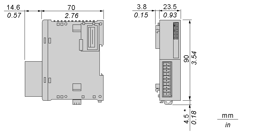
NOTE: * 8.5 mm (0.33 in) when the clip-on lock is pulled out.
TM2AMI4LT General Characteristics
|
Rated power supply voltage |
24 Vdc |
|
Power supply range |
19.2...30 Vdc including ripple |
|
Connector insertion/removal durability |
100 times minimum |
|
Internal 5 Vdc current draw |
50 mA |
|
Internal 24 Vdc current draw |
0 mA |
|
External 24 Vdc current draw |
60 mA |
|
Weight |
85 g (3 oz) |
TM2AMI4LT Input Characteristics
|
Characteristic |
Voltage input |
Current input |
Temperature probe input |
|---|---|---|---|
|
Input range |
0...10 Vdc |
0...20 mA |
(RTD) Pt 100, Pt 1000, Ni 100, Ni 1000 3-wire type Pt sensor -200...600 °C (-328...1112 °F) Ni sensor -50...150 °C (-58...302 °F) |
|
Input impedance |
> 10 kΩ |
< 250 Ω |
> 10 kΩ |
|
Sample duration time |
160 ms |
||
|
Total input system transfer time |
4x160 ms + 1 scan time |
8x160 ms + 1 scan time |
|
|
Input type |
Nondifferential |
||
|
Operating mode |
Self-scan |
||
|
Conversion mode |
ΣΔ type ADC |
||
|
Input tolerance - maximum deviation at 25°C (77°F) |
±0.2 % of full scale ± 0.4 % temperature probe input |
||
|
Input tolerance - temperature drift |
±0.005 % of full scale/°C |
||
|
Input tolerance - repeatable after stabilization time |
± 0.1% of full scale |
||
|
Input tolerance - nonlinear |
±0.02 % of full scale |
||
|
Input tolerance - maximum deviation |
±0.5 % of full scale |
||
|
Resolution |
12 bits (4096 increments) |
||
|
Input value of LSB |
2.5 mV |
4.8 μA |
K: 0.15 °C (K: 0.27 °F) |
|
Data type in application program |
0 to 4095 Scalable to -32768 to 32767 2 |
||
|
Input data out of range detection |
Yes3 |
||
|
Noise resistance - cable |
Twisted-pair shielded cable is necessary for improved noise immunity |
||
|
Noise resistance - external crosstalk |
1 LSB maximum |
||
|
Isolation between inputs, external power supply and internal logic circuits |
2500 Vac by photocoupler |
||
|
Isolation between inputs |
None |
||
|
Type of protection |
Photocoupler between input and internal circuit (1500 Vdc isolation) |
||
|
Maximum continuous allowed overload (no damage) |
13 Vdc |
40 mA |
− |
|
Selection of analog input signal type |
Using programming software NOTE: All inputs have the same voltage/current configuration or temperature. For temperature, it is possible to configure each channel independently of the type of probe. |
||
|
Calibration or verification to maintain rated accuracy |
Approximately 10 years |
||
|
Default input value in case of temperature sensor disconnectio |
Upper limit |
||
NOTE:
1.Total input system transfer time = sample repetition x 2 + 1 scan time.
2.The 12-bit data (0 to 4095) processed in the Analog I/O module can be linear-converted to a value between -32768 and 32767. The optional range designation and analog I/O data minimum and maximum values can be selected using data registers allocated to analog I/O modules.
3.When an input error is detected, a corresponding error code is stored to a data register allocated to analog I/O operating status.

