Characteristics of the TM2AMM6HT Module
This section provides a description of the electrical and the I/O characteristics of the TM2AMM6HT module.
|
|
|
CURRENT OVERLOAD AND FIRE POTENTIAL |
|
Select and install the appropriate wire size for the electrical current ratings of the I/O channels. |
|
Failure to follow these instructions will result in death or serious injury. |
|
|
|
UNINTENDED EQUIPMENT OPERATION |
|
Do not exceed any of the rated values specified in this chapter. |
|
Failure to follow these instructions can result in death, serious injury, or equipment damage. |
The following diagrams show the dimensions for the TM2AMM6HT analog I/O module.
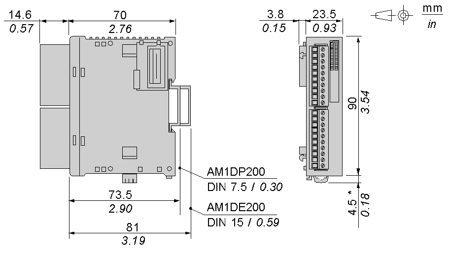
NOTE: * 8.5 mm (0.33 in) when the clip-on lock is pulled out.
TM2AMM6HT General Characteristics
|
Rated power supply voltage |
24 VDC |
|
Power supply range |
19.2...30 VDC including ripple |
|
Connector insertion/removal durability |
100 times minimum |
|
Internal 5 VDC current draw |
60 mA |
|
Internal 24 VDC current draw |
0 mA |
|
External 24 VDC current draw |
80 mA |
|
Weight |
85 g (3 oz) |
TM2AMM6HT Input Characteristics
|
Characteristic |
Voltage input |
Current input |
|---|---|---|
|
Input range |
0...10 VDC |
4...20 mA |
|
Input impedance |
1 MΩ min |
< 250 Ω |
|
Sample duration time |
64 ms max. |
|
|
Filtering |
It is possible to adjust by software the acquisition time for each channel from 16 ms to 64 ms. |
|
|
Total input system transfer time |
4 x 64 ms + 1 scan time (1) |
|
|
Input type |
Nondifferential |
|
|
Operating mode |
Self-scan |
|
|
Conversion mode |
ΣΔ type ADC |
|
|
Input tolerance - maximum deviation at 25°C (77°F) |
±0.5 % of full scale |
|
|
Input tolerance - temperature drift |
±0.015 % of full scale/°C |
|
|
Input deviation - repeatable after stabilization time |
±0.5 % of full scale |
|
|
Input tolerance - nonlinear |
±0.4 % of full scale |
|
|
Input tolerance - maximum deviation |
±1 % of full scale |
|
|
Resolution |
12 bits (4096 increments) |
|
|
Input value of LSB |
2.5 mV |
4.8 μA |
|
Data type in application program |
0 to 4095 Scalable to -32768 to 32767 (2) |
|
|
Input data out of range detection |
Yes3 |
|
|
Input protection |
Against reverse polarity and short circuit |
|
|
Noise resistance - maximum temporary deviation during perturbations |
±2 % of full scale |
|
|
Noise resistance - cable |
Twisted-pair shielded cable is necessary |
|
|
Noise resistance - crosstalk |
1 LSB maximum |
|
|
Isolation between inputs |
None |
|
|
Isolation between inputs and outputs, between inputs and external power supply |
800 VAC between inputs and outputs, between channels and PSU |
|
|
Isolation between inputs, power supply and internal logic circuits |
Photocoupler between input and internal circuit (1500 VAC) |
|
|
Maximum continuous allowed overload (no damage) |
30 VDC |
40 mA |
|
Selection of analog input signal type |
Choose current and voltage types using programming software |
|
|
Calibration or verification to maintain rated accuracy |
Approximately 10 years |
|
NOTE:
1.Total input system transfer time = sample duration time x active channel number + 1 scan time.
2.The 12-bit data (0 to 4095) processed in the Analog I/O module can be linear-converted to a value between -32768 and 32767. The optional range designation and analog I/O data minimum and maximum values can be selected using data registers allocated to analog I/O modules.
3.When an input error is detected, a corresponding error code is stored to a data register allocated to analog I/O operating status.
TM2AMM6HT Output Characteristics
|
Characteristic |
Voltage output |
Current output |
|---|---|---|
|
Output range |
0...10 VDC |
4...20 mA |
|
Load impedance |
2 kΩ minimum |
300 Ω maximum |
|
Application load type |
Resistive load |
|
|
Settling time |
20 ms |
|
|
Total output system transfer Time |
20 ms + 1 scan time |
|
|
Output tolerance - maximum deviation at 25°C (77°F) |
±0.9 % of full scale |
|
|
Output tolerance - temperature drift |
±0.015 % of full scale/°C |
|
|
Output deviation - repeatable after stabilization time |
±1 % of full scale |
|
|
Output tolerance - output voltage drop |
±1 % of full scale |
|
|
Output tolerance - nonlinear |
±0.5 % of full scale |
|
|
Output tolerance - output ripple |
±0.5% of full scale |
|
|
Output deviation - overshoot |
±0.5% of full scale |
|
|
Output tolerance - total deviation |
±1.5% of full scale |
|
|
Resolution |
12 bits (4096 increments) |
|
|
Output value of LSB |
2.5 mV |
4.8 μA |
|
Data type in application program |
0 to 4095 Scalable to -32768 to 32767 1 |
|
|
Noise resistance - maximum temporary deviation during perturbations |
±1 % of full scale |
|
|
Noise resistance - cable |
Twisted-pair shielded cable is necessary for improved noise immunity |
|
|
Noise resistance - crosstalk |
0.1% of full scale maximum |
|
|
Isolation between inputs |
None |
|
|
Isolation between outputs and external power supply |
800 Vac |
|
|
Isolation between outputs and outputs |
800 Vac |
|
|
Isolation between outputs and internal logic circuits |
Photocoupler between output and internal circuit (1500 Vac) |
|
|
Selection of analog output signal type |
Choose current and voltage types using programming software |
|
|
Calibration or verification to maintain rated accuracy |
Approximately 10 years |
|
NOTE:
1.The 12-bit data (0 to 4095) processed in the Analog I/O module can be linear-converted to a value between -32768 and 32767. The optional range designation and analog I/O data minimum and maximum values can be selected using data registers allocated to analog I/O modules.

