TM7SDM12DTFS Wiring
Connection Elements
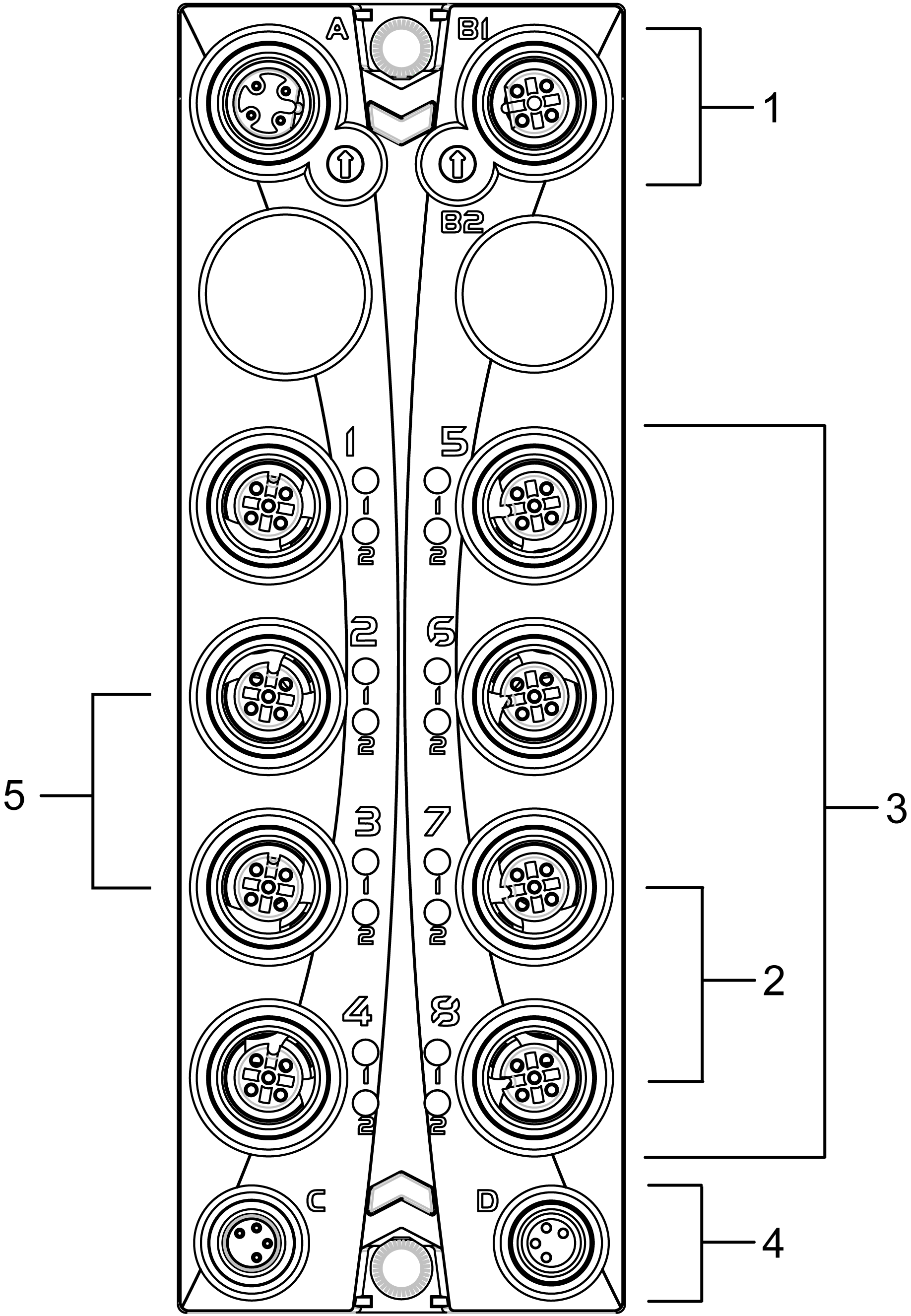
The following figure presents the connection elements for the TM7SDM12DTFS:
|
Number |
Meaning |
|---|---|
|
1 |
TM5 link:
|
|
2 |
SO4 is available on connectors 7 and 8 (physical connection) |
|
3 |
Digital I/O 8 x M12 (5-pin) |
|
4 |
Module supply 24 Vdc:
|
|
5 |
SI4 is available on connectors 2 and 3 (physical connection) |
Pin Assignments
The pin assignments of the power and communication connectors (A, B, C and D) are provided in the TM7 Physical Description.
The following figure presents the pin assignment for the TM7SDM12DTFS:
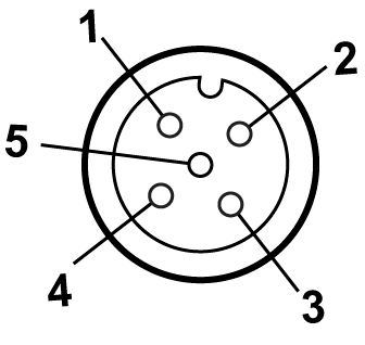
1 Test (pulse) x (inputs) or COM (outputs)
2 SI x (safety-related inputs) or SO x (safety-related outputs)
3 COM
4 SI y (safety-related inputs) or SO y (safety-related outputs)
5 Test (pulse) y (inputs) or COM (outputs)
The following table describes the pin assignments for the inputs of TM7SDM12DTFS (N.C. = No Connection):
|
Connector socket |
Pin1 |
Pin2 |
Pin3 |
Pin4 |
Pin5 |
|---|---|---|---|---|---|
|
1 (IN) |
Test (pulse) 1 |
SI 1 |
COM |
SI 2 |
Test (pulse) 2 |
|
2 (IN) |
Test (pulse) 3 |
SI 3 |
COM |
SI 4 |
Test (pulse) 4 |
|
3 (IN) |
N.C. |
N.C. |
COM |
SI 4 |
Test (pulse) 4 |
|
5 (IN) |
Test (pulse) 5 |
SI 5 |
COM |
SI 6 |
Test (pulse) 6 |
|
6 (IN) |
Test (pulse) 7 |
SI 7 |
COM |
SI 8 |
Test (pulse) 8 |
The following table describes the pin assignments for the outputs of TM7SDM12DTFS (N.C. = No Connection):
|
Connector socket |
Pin1 |
Pin2 |
Pin3 |
Pin4 |
Pin5 |
|---|---|---|---|---|---|
|
4 (OUT) |
COM |
SO 1 |
COM |
SO 2 |
COM |
|
7 (OUT) |
COM |
N.C. |
COM |
SO 4 |
COM |
|
8 (OUT) |
COM |
SO 3 |
COM |
SO 4 |
COM |
| WARNING | |
|---|---|
| WARNING | |
|---|---|
Detected errors are acknowledged in a similar way. As soon as a detected channel error has been acknowledged, the error state on the other channel of the same connector is also acknowledged.
However, the restart inhibit is separately active for each channel to help prevent unintentional enabling of a channel.
| WARNING | |
|---|---|
| WARNING | |
|---|---|